※〔EXHIBITION NEWS〕Global Advanced Packaging Accelerates Growth, E&R Showcases Latest Laser and Plasma Solutions at SEMICON Taiwan 2025
As AI, high-performance computing (HPC), and 5G drive continuous breakthroughs in semiconductor manufacturing, advanced packaging has become the next strategic focus. According to Yole Group, the global advanced packaging market is set to expand at a CAGR of 8–10%, exceeding USD 50 billion by 2025. Fan-out panel-level packaging (FOPLP), in particular, is projected to grow more than 15% annually, driven by cost and yield advantages.
E&R Engineering (TPE: 8027) will showcase its latest laser and plasma solutions at SEMICON Taiwan 2025, covering FOPLP, Through-Silicon Via (TSV), Through-Glass Via (TGV), and plasma dicing. By delivering fully integrated process technologies, E&R enables customers to address critical challenges such as high I/O density, warpage control, and ultra-fine feature processing.
FOPLP Solutions
E&R offers a complete FOPLP equipment portfolio, including laser marking, dicing, plasma cleaning, laser debonding, and ABF drilling, supporting panel sizes from 300×300 mm to 700×700 mm. With modular design and precision control, the systems boost productivity while stably processing substrates with up to 16 mm warpage—demonstrating industry-leading manufacturability.
TSV – Through-Silicon Via Applications
With the growth of 3D packaging and advanced memory, TSV technology has become a key enabler for high-density integration. E&R provides end-to-end TSV solutions for via drilling, cleaning, and debonding. By combining laser and plasma processes, the systems deliver precise via profiles, low defectivity, and excellent interconnect reliability across multiple wafer sizes and materials.
Glass Substrate Solutions
In the emerging glass core substrate segment, E&R’s self-developed laser modification technology achieves >0.9 via circularity, aspect ratios up to 10:1, and drilling speeds of 1,500 vias/sec. The solution supports CoPoS and ABF substrate applications, enabling high-performance, high-yield glass substrate manufacturing. In partnership with E-core partners, E&R will also showcase a complete metallization-enabled glass substrate process flow at the show.
Advanced Packaging and Process Solutions
Designed, manufactured, and qualified in Taiwan with components from leading U.S. and European suppliers, E&R equipment has shipped over 500 units worldwide. Its solutions are widely adopted in FCBGA, FCCSP, fan-out, and wafer-level packaging by major OSATs and IDMs. The company also expanded its Flip Chip BGA portfolio, offering Pre-Flip Chip Die Bond Plasma Cleaning, Pre-Molding/Underfill Plasma Cleaning and Laser Marking for traceability. In 2025, E&R introduced a fully automated high-power burn-in solution, supporting up to 3,000W test environments.
E&R invites industry partners to visit SEMICON Taiwan 2025 and explore next-generation packaging and dicing technologies with our technical team.
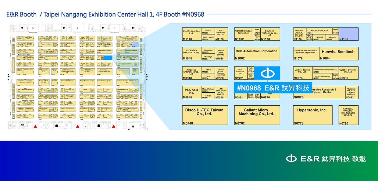
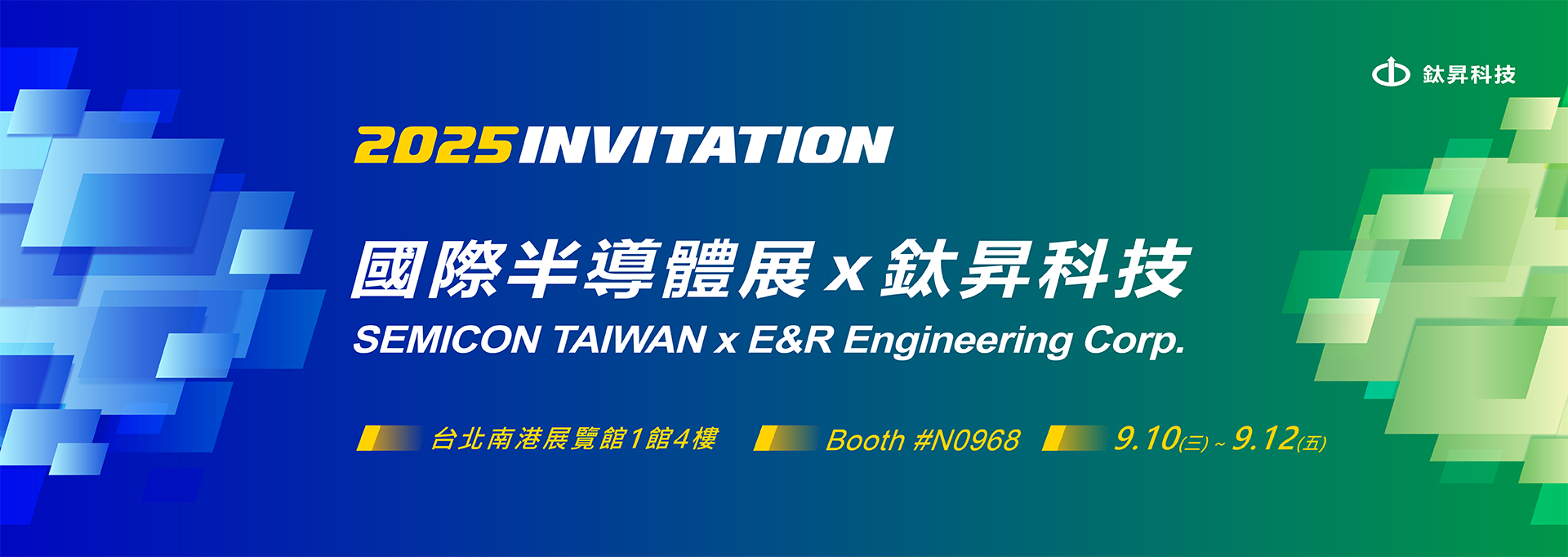
E&R Booth Information
Location: Taipei Nangang Exhibition Center Hall 1
Booth Information: 4F, #M120
Date: April 16 (Wed.) -18 (Fri.), 2025