

E&R Engineering to Launch New Malaysia Plant: Expanding Global Packaging Materials Production and Localized Services
[Kaohsiung, Taiwan]
E&R Engineering Corp., an international provider of semiconductor packaging equipment, announced today the upcoming grand opening of its new Malaysian subsidiary—E&R SEMICONDUCTOR (MALAYSIA) SDN. BHD.—at the Melaka Free Trade Zone on October 13.
To meet surging Southeast Asian demand, E&R Engineering is upgrading its global strategy for the packaging materials business unit. While its plant in China continues to experience steady business growth, E&R is strategically shifting a portion of its production focus to Malaysia while simultaneously expanding overall capacity. The new facility is currently undergoing sample testing and qualification, with mass production scheduled to officially begin early next year. The plant is expected to create 50 local job opportunities, driving regional economic and industrial development. This expansion will further strengthen E&R’s supply capabilities in Southeast Asia, delivering real-time technical support and supply chain flexibility to semiconductor and OSAT (Outsourced Semiconductor Assembly and Test) customers.
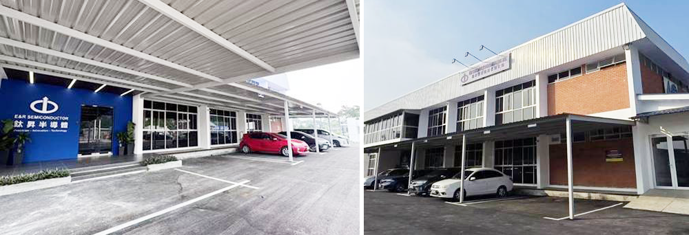
AK Ong, General Manager of the Malaysia plant, added: "The completion of our new facility allows us to stay closer to our customers, offering real-time support and superior service. We remain committed to delivering top-quality products and strictly monitoring every quality checkpoint to create a win-win future for all."
[Event Details]
E&R Engineering Corp., an international provider of semiconductor packaging equipment, announced today the upcoming grand opening of its new Malaysian subsidiary—E&R SEMICONDUCTOR (MALAYSIA) SDN. BHD.—at the Melaka Free Trade Zone on October 13.
To meet surging Southeast Asian demand, E&R Engineering is upgrading its global strategy for the packaging materials business unit. While its plant in China continues to experience steady business growth, E&R is strategically shifting a portion of its production focus to Malaysia while simultaneously expanding overall capacity. The new facility is currently undergoing sample testing and qualification, with mass production scheduled to officially begin early next year. The plant is expected to create 50 local job opportunities, driving regional economic and industrial development. This expansion will further strengthen E&R’s supply capabilities in Southeast Asia, delivering real-time technical support and supply chain flexibility to semiconductor and OSAT (Outsourced Semiconductor Assembly and Test) customers.
Deepening Roots in Southeast Asia’s Packaging Hub: Localized Mass Production of Advanced Carrier Tapes
Accounting for approximately 13% of the world's backend packaging and testing capacity, Malaysia's semiconductor market is projected to reach $16.51 billion by 2030, driven by robust policy support. Capitalizing on this strong momentum and increasing regional customer demand, E&R has established a forward-looking footprint in Phase III of the Batu Berendam Free Trade Zone in Melaka. The facility brings its years of core manufacturing expertise in high-end Embossed Carrier Tapes and Cover Tapes directly to local production. Through "local manufacturing and fast response," the new plant directly addresses OSAT and semiconductor giants' needs—significantly shortening lead times while providing high precision, excellent electrostatic discharge (ESD) protection, and robust packaging interfaces to support advanced packaging trends like chip miniaturization and Chiplet integration.Opening a New Chapter with "Innovation, Collaboration, and Growth"
E&R Engineering President KS Chen stated: "The inauguration of our Malaysia plant marks a milestone in the global deployment of our carrier tape business. To address growing customer demand in Southeast Asia, we have shifted part of our production focus to Malaysia while expanding our capacity. Furthermore, this facility serves as a dedicated local hub for E&R's semiconductor equipment engineers and Field Service Engineers. We will focus on hiring local talent and building our specialized equipment engineering team, enabling us to provide immediate, localized technical support and equipment services, thereby enhancing customer satisfaction and trust. "AK Ong, General Manager of the Malaysia plant, added: "The completion of our new facility allows us to stay closer to our customers, offering real-time support and superior service. We remain committed to delivering top-quality products and strictly monitoring every quality checkpoint to create a win-win future for all."
[Event Details]
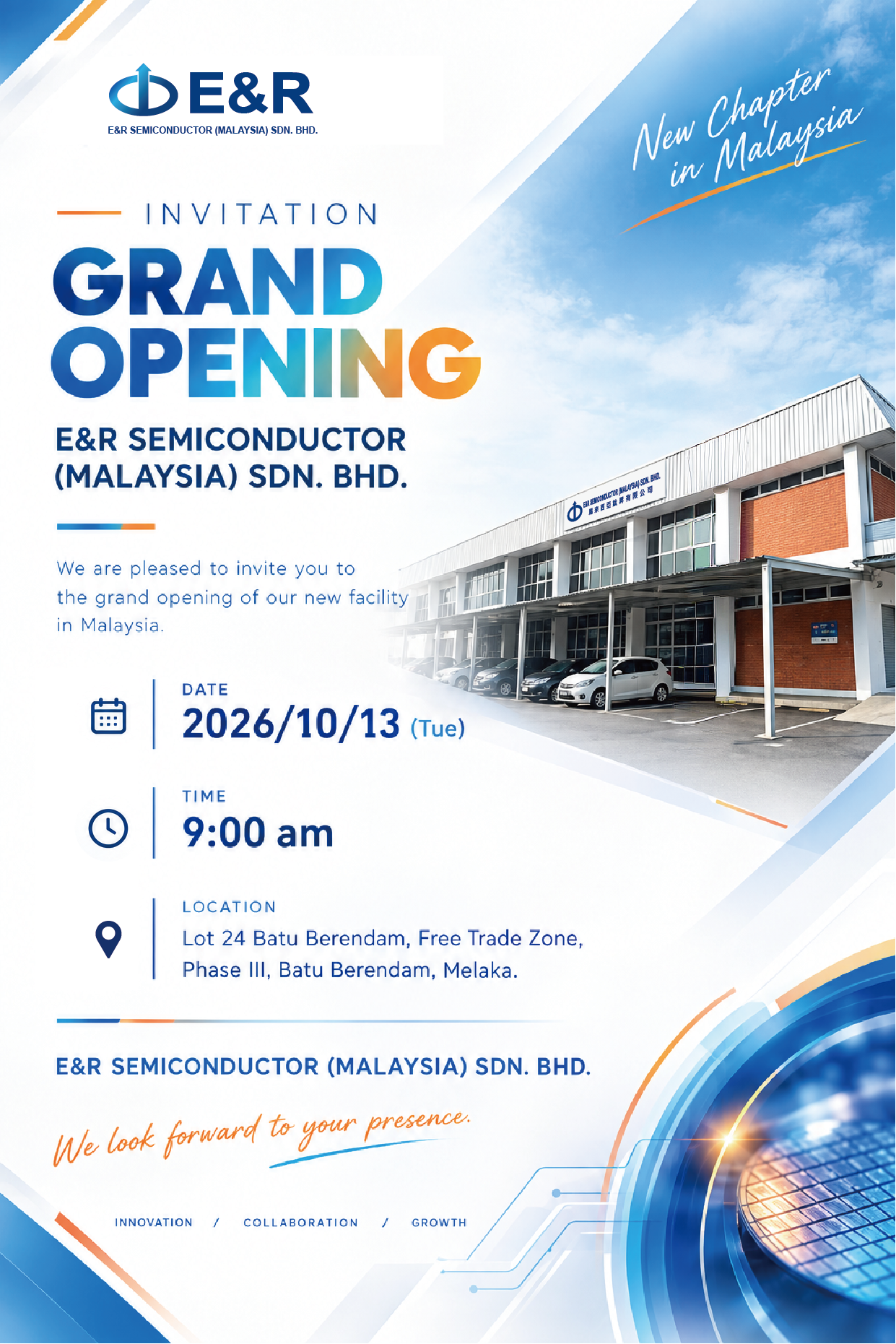
- Event: E&R Semiconductor (Malaysia) Sdn. Bhd. Grand Opening Ceremony
- Date: Tuesday, October 13, 2026
- Time: 09:00 AM
- Location: Lot 24 Batu Berendam, Free Trade Zone, Phase III, Batu Berendam, Melaka, Malaysia
2026-10-04