
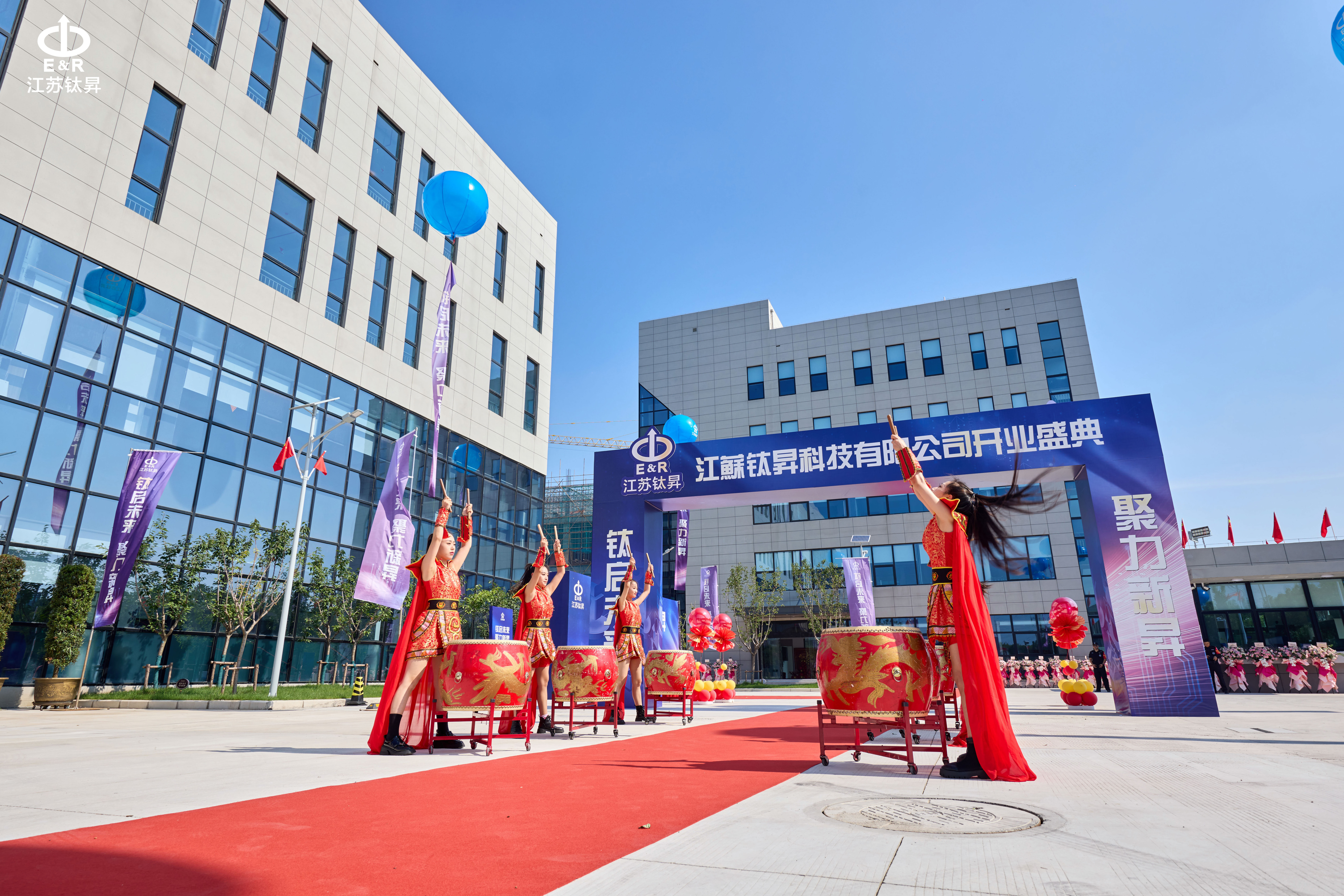
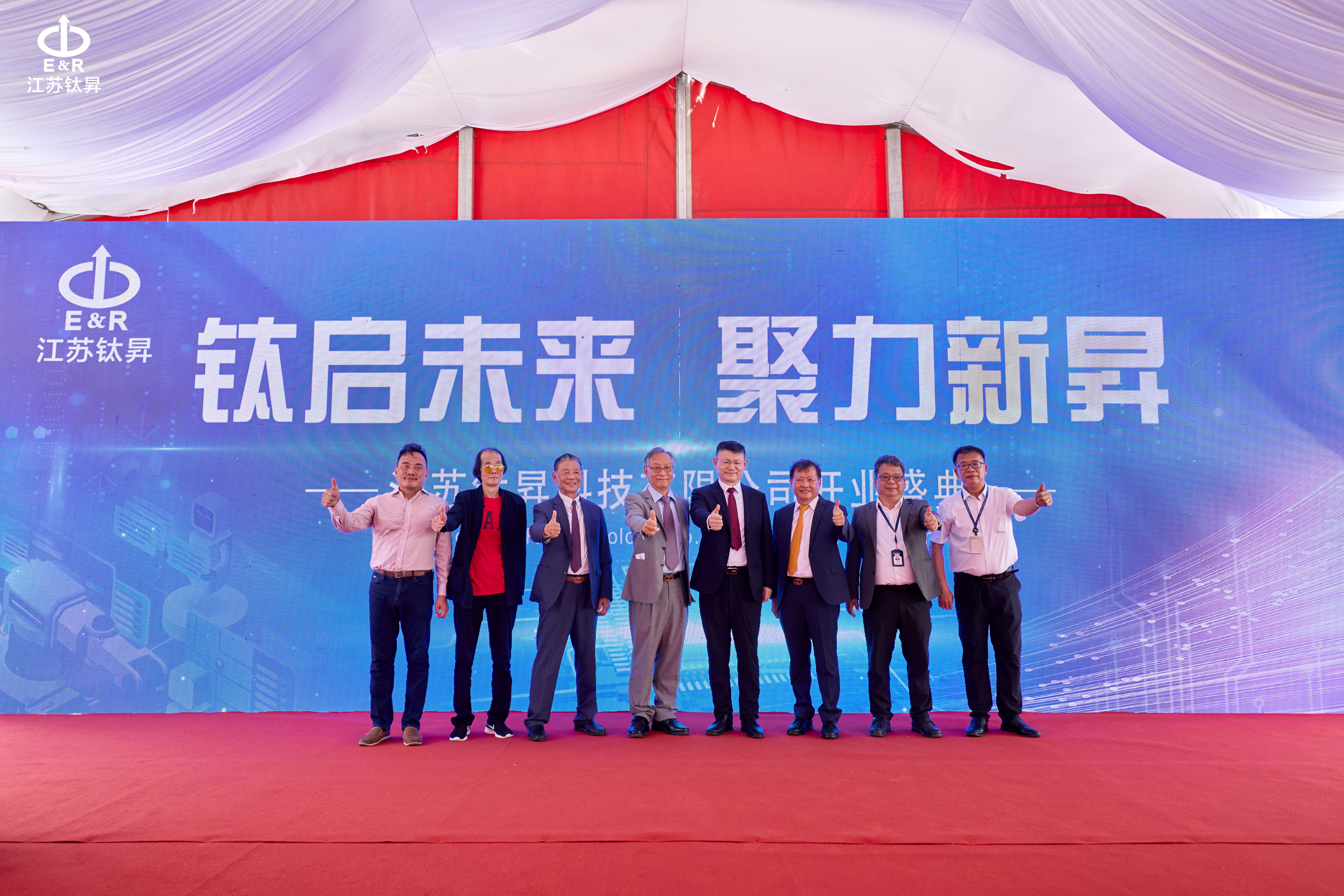
Inauguration Ceremony of E&R in Jiangsu, July 4th, 2024.
(Executive Vice Chairman of E&R, Mr. KS Chen,CEO of Jiangsu E&R, Mr. Harry Huang, President of E&R, Mr. Eric Chang warmly welcome all distinguished guests to the opening ceremony of E&R Technology's new factory in Nantong.)
E&R's new factory in Nantong commenced operations, upholding the principles of "innovation, pragmatism, cooperation, and mutual benefit" to support global semiconductor development.
E&R, a manufacturer of advanced laser and plasma equipment, officially announced the opening of its new facility in Nantong, Jiangsu on July 4, 2024. During the opening ceremony, leaders from the Nantong Economic and Technological Development Zone, entrepreneurs from both sides of the Taiwan Strait, and senior executives led by Chairman Mr. Michel Wang were invited to attend, witnessing a new chapter in E&R's history. With the formal launch of the Nantong factory, E&R expects increased production capacity and enhanced global market competitiveness in the manufacturing of laser and plasma equipment, as well as electronic carriers.
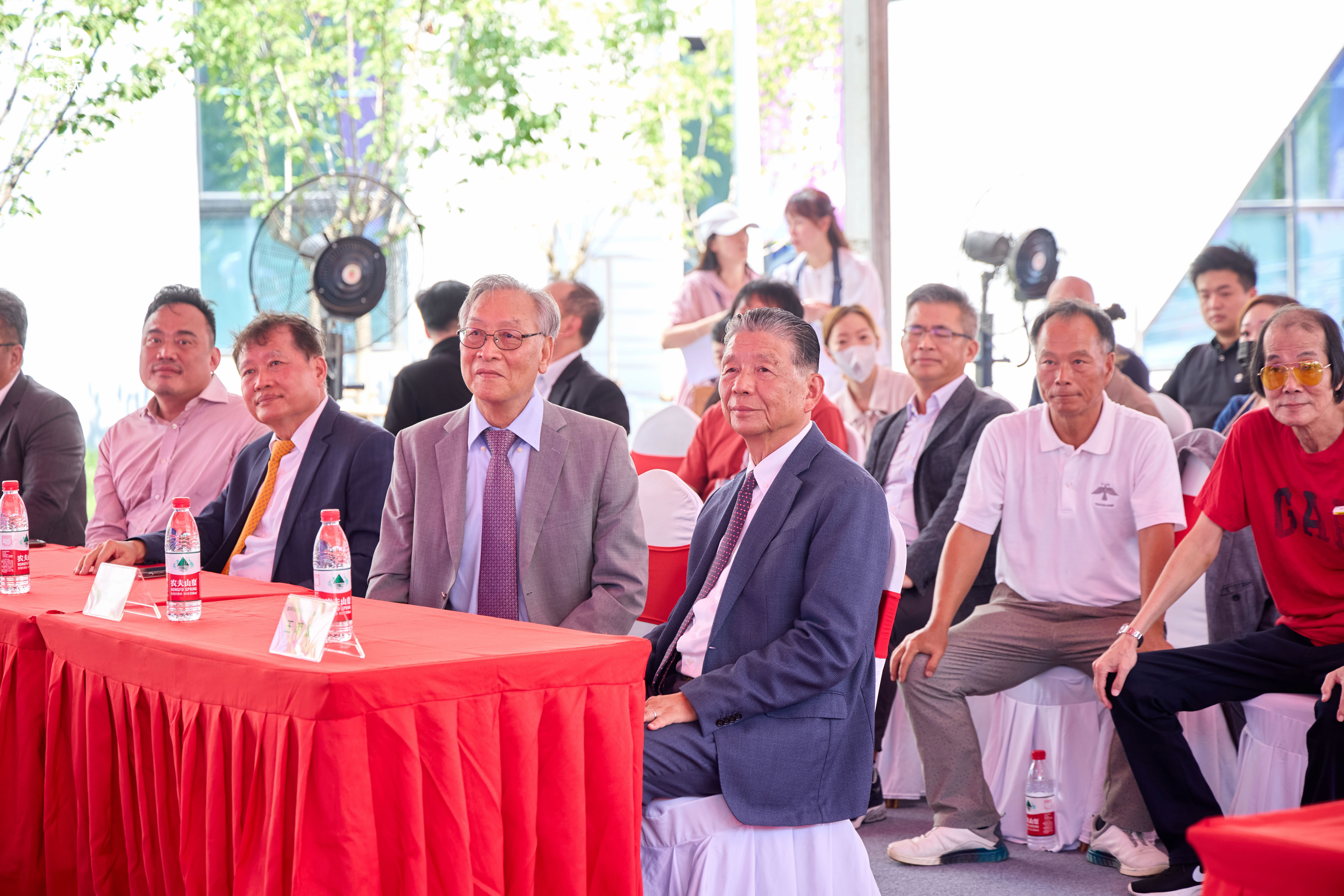
(In the front row, from left to right, are CEO of Jiangsu E&R, Mr. Harry Huang, President of E&R, Mr. Eric Chang, Executive Vice Chairman of E&R, Mr. KS Chen, Chairman of E&R, Mr. Michel Wang.)
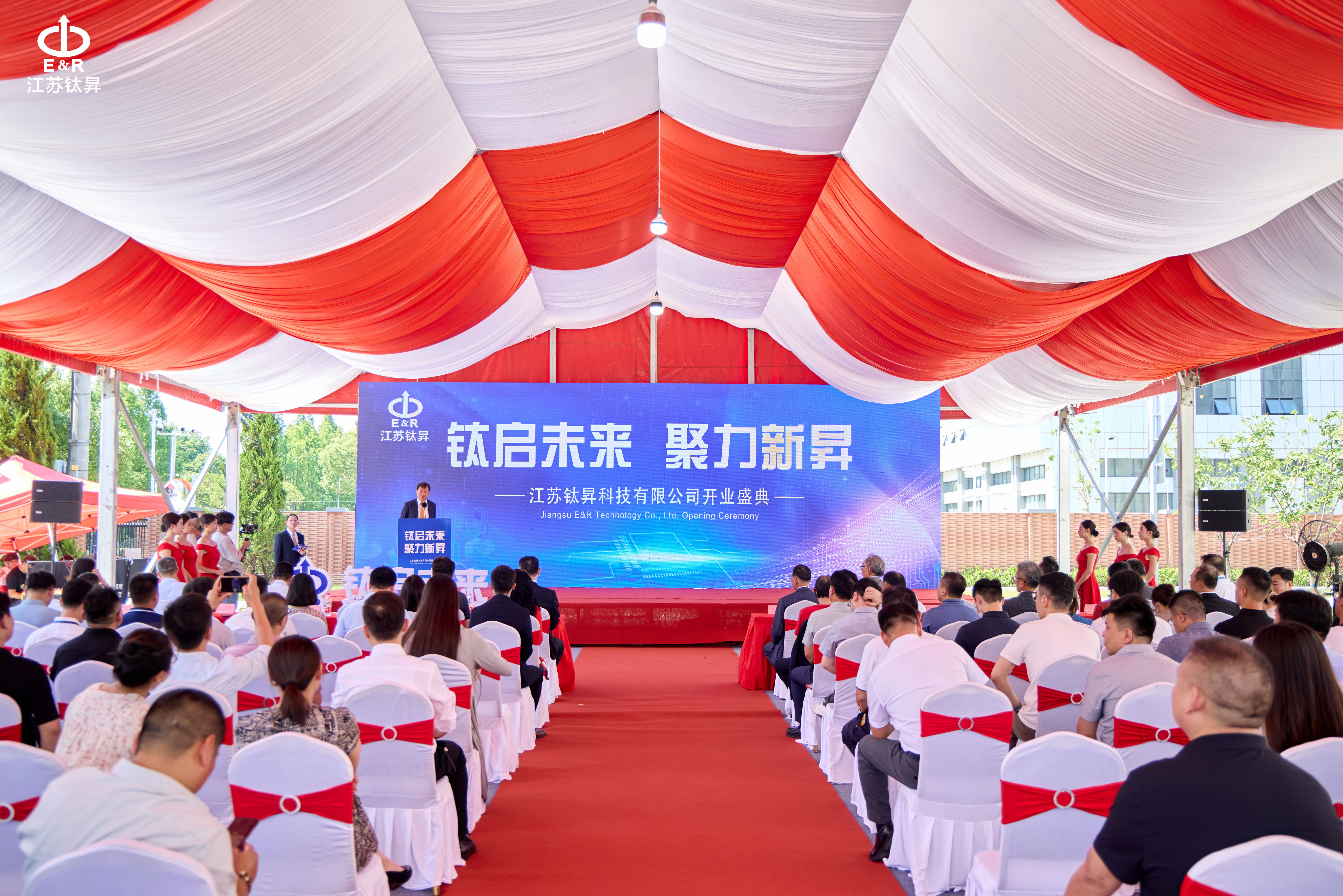
(President of E&R, Mr. Eric Change delivering a speech on stage.)
President of E&R, Mr. Eric Chang stated, "The completion of the Nantong factory not only provides us with a production base but also embodies our capabilities in technology research and development and innovation. We will establish a dedicated semiconductor plasma cutting production line here, specializing in RFID (radio frequency identification) technology, aiming to contribute to the advancement of semiconductor advanced packaging technology, artificial intelligence (AI), and smart labels."
CEO of Jiangsu E&R, Harry Huang remarked, "From nothing to something, we have established this iconic new factory in the midst of grasslands, hoping to inject new vitality into the economic and industrial development of the development zone. We will continue to strengthen cooperation with governments at all levels and partners to jointly promote the healthy development of the industry chain and achieve mutual benefit and win-win results."
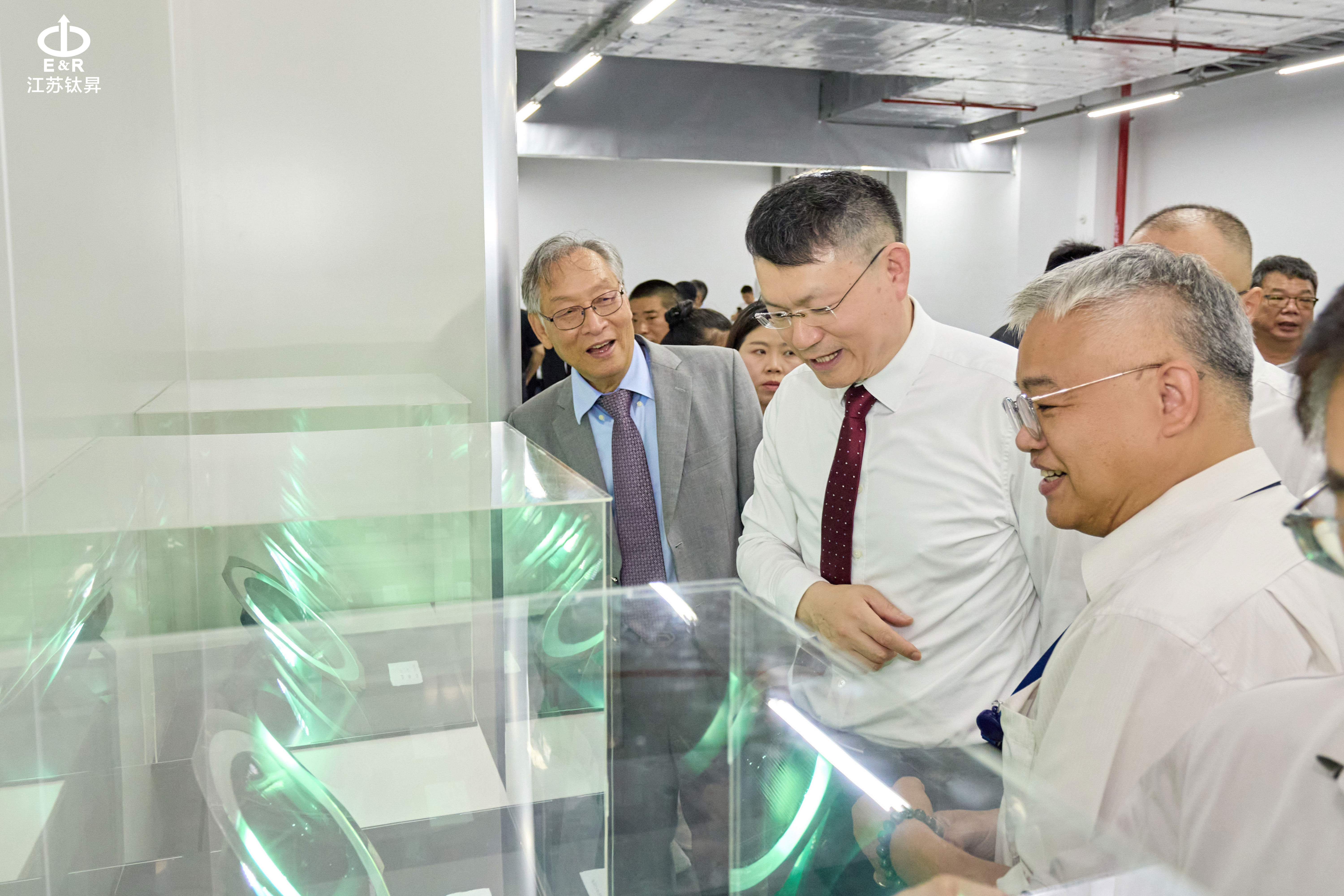
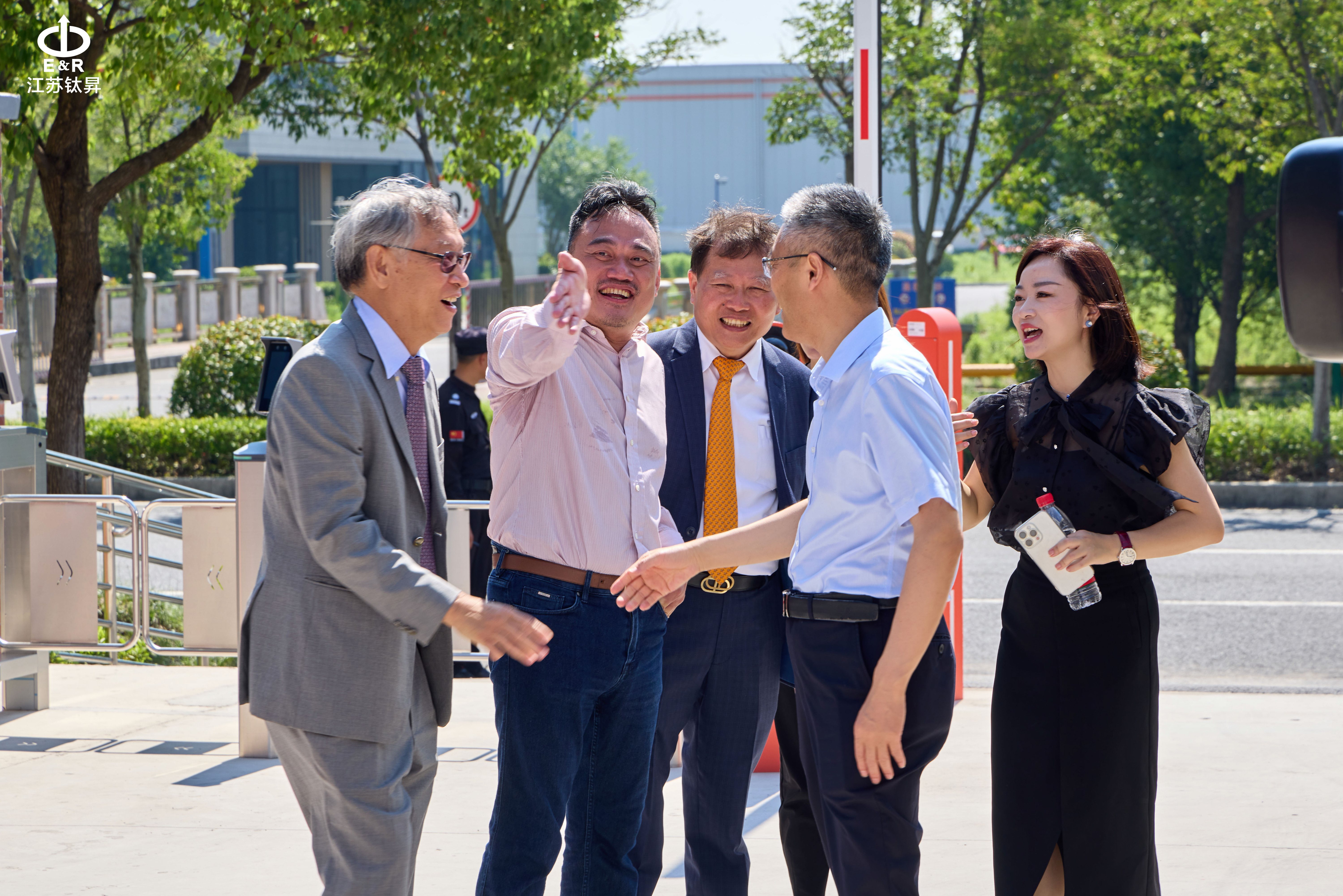
(Executive Vice Chairman of E&R, Mr. KS Chen led the guests on a tour of the Nantong factory.)
E&R's new factory in Nantong will also provide comprehensive one-stop plasma cutting services from wafers to chips, with an initial production capacity expected to reach 2,500 wafers per month. By 2025, after the completion of the entire production base construction, capacity is expected to increase significantly. E&R has been specializing in plasma cutting technology for several years, achieving chip cutting sizes smaller than 0.5 x 0.5 millimeters with cutting precision controlled between 10 to 30 microns, improving process yield compared to traditional wheel blade cutting.
After 30 years of dedication to the semiconductor industry, E&R has become an important player in the global artificial intelligence (AI) wave. Their advanced laser and plasma technologies are not only adopted by leading global IDMs but also closely cooperate with global packaging and foundry giants. Additionally, E&R has introduced numerous process technologies on new-generation glass substrates, establishing a leading position in TGV (Through Glass Via) equipment processes.In addition to focusing on research and development, E&R also adheres to the concept of green development, promoting energy conservation, emissions reduction, and environmental protection, fulfilling its commitment to sustainable operations.